Park XE7 (Direct On-Axis Manual Focus Optics)
The atomic force microscope (AFM) is extensively used in material science and biological sciences. Characterization of sol-gel thin film surface morphology in sub-micron scale is necessary to evaluate their function properties in a wide variety of applications. It has been known that sub-micron and nanoscale properties control various aspects of functional performance. For example, enhanced transmittance in borosilicate glass (BSG, 91%) over soda lime glass (SLG, 89%) is due to sub-nanometer surface morphology of BSG. This may occur due to its different chemical composition though the refractive indices are comparable.
Centre for Sol-Gel Coatings (CSOL)
Dr. K. Murugan

CS - 444, LECO, USA
Carbon/Sulphur system is a microprocessor based software driven instrument for wide range measurement of Carbon and Sulphur content of metals, ores, ceramics and other inorganic materials. It uses HF-400 induction furnace (18 MHz, 2,2 kW) for CO2/SO2 conversion. It works on the principle of infrared absorption of CO2 and SO2.
Centre for Nanomaterials (CNM)
Dr. Malobika Karanjai

CCX 2000, Atlas Material Testing Solutions, USA
To better understand the potential for adverse effects of outdoor exposure, materials are regularly tested to various environmental conditions. The cyclic corrosion cabinet is now accepted as superior at duplicating actual environments. It improves repeatability, reduces time spent in handling samples and also operator error by creating different environments in one cabinet. Standard exposure cycles like salt or chemical fog, water fog, salt spray, dry-off cycle, high temperatures i.e. up to 70oC can be increased for required time from hours to number of days which are closer to environmental changes.
Salient features-Materials of different sizes and shapes can be tested under various environmental conditions by using various standard methods like ASTM B117, ASTM G85 A5, CCT I, CCT IV, SAE J2334 and GM9540B.

SI 1287 ELECTROCHEMICAL INTERFACE
SI 1260 FREQUENCY RESPONSE ANALYSER
SOLARTRON ANALYTICAL (UK)
The electrochemical testing system consists of two units. Electrochemical interface and impedance/gain-phase analyzer along with softwares corroware and Z plot

SI1287-Solartron, U.K
The corrosion is an electrochemical process and electrochemical potential is the driving force for reactions. The principle employed in the electrochemical interface is based on the application of a controlled voltage to a sample (working electrode) and measurement of the change in current, or vice versa. The corrosion rates of the specimens can be determined using CorrWare programme. Most of the corrosion types uniform, localized, galvanic, dealloying; stress corrosion and hydrogen-induced failure can be analyzed by this technique. Conventional electrochemical experiments like static, dynamic polarization, potentiostatic, potentiodynamic experiments etc. can be done. This system is extensively used to study the corrosion properties of coated substrates. Based on the results, further improvement of coatings has been done. Different types of coatings like DLC on Al alloys, MAO coatings on Al, Coating on steels and Al alloys by Sol-Gel technique, materials like Mg-Zn, steels, alloys have been analyzed. The system can also be used to study batteries, fuel cells, inhibitors, electroplating and catalytic properties etc.
SI1260-Solartron, U.K
Frequency range 10 µHz to 32 MHz with 10 µHz resolution.
Electrochemical Impedance Spectroscopy is a powerful technique, which can provide lot of information on corrosion reactions, mass and charge transport, the characteristics of material and coating in different electrolytes. An electrode interface undergoing an electrochemical reaction is typically analogous to an electronic circuit consisting of a specific combination of resistors and capacitors. This is used to characterize the electrochemical system in terms of its equivalent circuit. The system is widely used in characterization of materials, batteries, and coatings and to illustrate their corrosion mechanism. It is also used for investigating mechanisms in electrodeposition, electrodissolution, passivity and corrosion studies.
Centre for Material Characterization and Testing (CMCT)
Ms. A. Jyothirmayi
Vertex 70; Bruker Optik GmbH, Germany
The equipment enables optical and thermal emittance characteristics (Transmittance, spectral emittance and thermal emissivity) of solar absorber materials and coatings especially employed in the field of solar thermal applications. Also it enables all the basic characterisations of chemical compounds in the form of solids, liquids and low temperature crystalline. It is widely applied in solar thermal, Solar PV and chemical analysis
Centre for Solar Energy Materials (CSEM)
Dr. S. Sakthivel
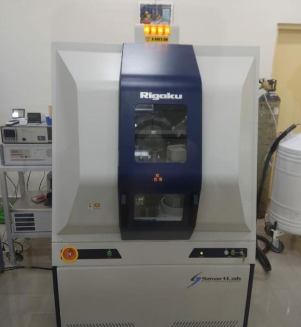
SmartLab 2018, Rigaku, Japan
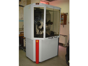
High Flux X-ray diffraction (XRD) unit is equipped with 9kW rotating Cu anode which provides nearly one order higher flux on the sample than the sealed tube X-ray source. This XRD machine can be used to carry out angular dispersive scans with 2 from 5 to 160 deg. and an angular resolution of 0.01 degrees. Specially designed sample holders are available for mounting of solid samples and powder samples. With aid of auto sampler robot, a maximum of 48 powder and 24 bulk samples can be measured with operator intervention.
Centre for Materials Characterization and Testing (CMCT)
Dr. K. Suresh
Micro Materials Ltd., Wrexham LL13 7YL, UK
Nanotest Vantage (Alpha) with NTX4 Contoller
Centre for Materials Characterization and Testing (CMCT)
Dr. P. Suresh Babu
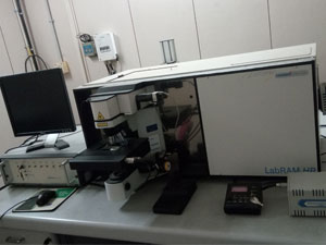
Horiba Jobin Yvon; Labram Micro Raman Spectrometer
Raman Spectrometery is complementary to FTIR. Raman can be used to analyse aqueous solutions since it does not suffer from the large water absorption effects found with FT techniques. Raman requires little or no sample preparation. Raman Spectroscopy actually originates from the bond vibrations. This intrinsic nano probing combined with micro raman spectroscopy makes it very sensitive to short range structure in the nano materials. Thus it is good complement to TEM or X-Ray Diffraction techniques. The advantage of No sample preparation required both for solid and liquid samples in Micro Raman Spectroscopy makes it an easy access to characterize nano materials. Micro Raman provides phase identification, even traces of secondary phase can be detected as the polarisibility changes for different kinds of bonds which is detected in the Raman intensity.
Centre for Nanomaterials (CNM)
Dr. B.V. Sarada
With the aid of computer control, arrays of indents can be made on the sample and the hardness can be measured as a function of distance from a reference point. This unit is especially suitable to induce cracks on the sample surface so that the fracture toughness can be measured.
Centre for Materials Characterization and Testing (CMCT)
Dr. L. Venkatesh

RAPID-II-D/MAX MICROFOCUS X-ray Diffraction System (RIGAKU Corp., Japan)
This is the most versatile laboratory scale x-ray diffraction system. It is equipped with high intensity microfocus rotating anode x-ray source-Rigaku MicroMax 007HF, which has brightness close to a second generation synchrotron with x-ray flux of 1014 to 1015 x-ray photon/mm2/s at the focal point. The system also has a highly sensitive and large image plate based 2-dimensional (2D) detector, which ensures a full scan from -47 to +163 degree for 2theta in a single exposure of very small duration. It has both Cu and Cr target option with provision to bring the beam spot size down to 10 micron. The system can be operated in reflection, transmission and glancing incidence configuration. It can perform wide range of studies like phase analysis, texture, residual stress, trace phase detection (for phase fraction of 0.1% or less) in micro/macro-area apart from thin film analysis in the glancing incidence mode. In addition, it has a provision to perform fully automated area mapping using auto stage.
Centre for Nanomaterials (CNM)
Dr. Joydip Joardar

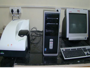
Nano SZ, Malvern Instruments Limited, UK
The instrument measures the diffusion coefficient (D) and converts this to particle size, using the Stokes-Einstein equation: D=kT/3S, D=Hydrodynamic diameter, T=Absolute temperature, D=Diffusion Coefficient, K=Boltzman's constant, =Viscosity/c
Centre for Ceramic Processing (CCP)
Dr. Buchi Suresh
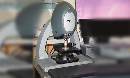
The system is used for estimating surface roughness and other surface parameters, as also to create 3D profiles of surfaces. It uses white light interferometry to map specimen surfaces. A beam splitter is used to split the incoming beam into two. One part goes to a reference mirror that is optically smooth while the other part scans the sample surface. The interference pattern between the two beams (that is, the one coming from the reference mirror and the other from the sample) is used to recreate the surface profile. The resolution of the unit is 0.1 nm and hence optically smooth surfaces can be studied. An advantage of this system over an atomic force microscope is that there is no mechanical contact with any part of the sample and hence even smooth and soft surfaces can be profiled. Another advantage is that the optics stay much above the sample and hence even deeper areas of the sample surface can be imaged as far as the light beam is able to fall on the area of interest.
Centre for Materials Characterization and Testing (CMCT)
Dr. L. Venkatesh
MS3000, Malvern Instruments Ltd., UK
Measures particle size distribution and size
Centre for Ceramic Processing (CCP)
Dr.Buchi Suresh
X'pert Pro residual analyser
The unit is used for estimating residual stresses in the coatings and other surfaces using X-ray diffraction. Since stress is an intrinsic property it cannot be directly measured. The basic principle is that the strain in a system can be found out by measuring the interplanar spacing 'd' and calculating the stress from a series of equations. The X'pert Pro residual stress analyser available with the centre works with a Cu source for x-rays. It has a five-axis goniometer. The main application of this technique is the measurement of stress by non-destructive means. Apart from residual stress analysis, glancing angle measurements, texture measurements and phase analysis can also be carried out.
Centre for Engineered Coatings (CEC)
Dr. N. Ravi

This instrument is used for studying sample surfaces at high magnifications (> 200000x) due to the presence of a hot Schottky field emission (FE) gun. Potential (called the extraction voltage) is applied to draw out the electrons. Due to this combination of high temperature and extraction voltage, the brilliance of the source beam, as also its stability, is high. This system is attached with an EDS unit and an electron back scatter diffraction (EBSD) unit.
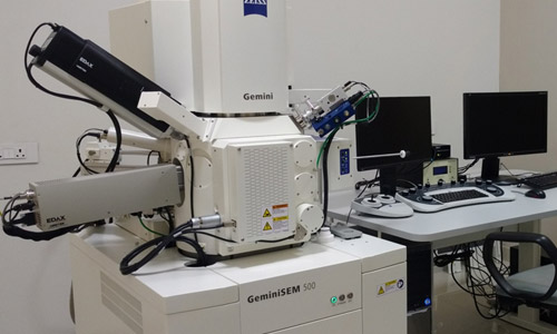
One of the interactions that occur when an incident electron beam falls on a sample is the production of x-rays from the sample. The x-ray frequency is characteristic of the element in the sample that produces it. Thus, several elements can be analysed simultaneously. The detector analyses the energies of the generated x-rays, leading to speedy detection of the elements.
In the EBSD unit, the sample is kept inclined at an angle of 70 to the incident beam and the emergent backscattered electrons undergo diffraction. The diffracted beams are collected on a phosphor screen where they form bands that are indexed based on known crystallographic inputs. The electron beam moves on the sample surface in a regular manner based on a step size determined by the user. Electron diffraction occurs at each point and the entire area of interest on the sample surface is mapped. EBSD is a technique where the input is crystallographic information and the output is microstructural information. The orientation of individual grains can be measured using EBSD, as also the grain shape, size and boundary statistics. EBSD is also a powerful tool for the determination of crystallographic texture. A special feature of the unit at ARCI is that the EDS and EBSD units work in synchronisation and hence elemental and microstructual information can be collected from each point from the area of interest. A recent area of application is phase analysis using the EDS/EBSD combination. Since spatial information from the different grains is preserved in EBSD, the location of small amounts of secondary phases (at triple points or within grains) can be determined accurately.
Centre for Materials Characterization and Testing (CMCT)
Dr. L. Venkatesh
STA 449 Jupiter - Netzsch GmbH, Germany
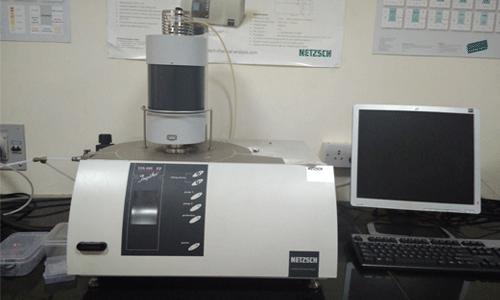
Measures TGA/DTA and DSC simultaneously from room temperature to 1400 C.
In STA, the sample is subjected to a controlled temperature programme of heating where the change in mass, the absolute sample temperature and the difference in temperature of sample with a reference are measured simultaneously and monitored very accurately. With a proper calibration the heat flux to and from the sample can be calculated which in turn helps in determining the specific heat as a function of temperature. The specific heat of a material is an important thermodynamic parameter which helps to study and understand the mechanism of phase transitions etc.
Centre for Carbon Materials (CCM)
Dr. P.K. Jain
ASAP 2020
Surface area and porosity are two important physical properties of the nanopowders that can be measured by this method. The equipment works on gas absorption principle therefore, it is very effective tool to study the surface morphology of the materials. Surface area (as low as 0.05m2/g) can be measured. It can measure adsorption and desorption isotherms to determine the shape of pores. It is possible to carryout measurements using adsorbates such as N2, Ar, CO2 and Kr selectively and also capable of measuring Langmuir surface area and pore size distribution. Volume, area, total pore volume and pore size in the range 0.35 to 500nm can be determined.
Centre for Nanomaterials (CNM)
Dr. Neha Yeshwanta Hebalkar

Small-angle X-ray scattering (SAXS) ,Xenocs, France
A laboratory small-angle X-ray scattering (SAXS) system with a dual energy (Mo and Cr) source has been designed with the aim of studying the heterogeneity in high-Z metallic structural materials such as steels (Fe alloy) and other materials. With the combination of Mo and Cr energies, various camera lengths (maximum of 2400 mm), and an area detector, three decades of q range has been achieved, from 0.024 to 14 nm-1. In real space, the probing periodic distance is a maximum of 261 nm. In addition to having Mo and Cr sources, a flexible sample mounting stage permits measurements on a wide range of materials in transmission geometry. More details about instrument can be found at “A multi-functional dual-energy laboratory Mo-Cr-SAXS system” J. Appl. Cryst. (2015). 48, 2040-2043 https://doi.org/10.1107/S1600576715018804 http://scripts.iucr.org/cgi-bin/paper?S1600576715018804

Centre for Materials Characterization and Testing (CMCT)
Dr. K. Suresh
F20, Filmetrics Inc., USA
The thin film analyzer works based on the intensity measurement of reflecting and transmitting light through the sample. Hence, thickness of only transparent coatings can be measured, though the substrates can be of transparent or non-transparent nature. There are possibilities of using a contact or a non-contact probe depending upon the nature of film and the substrate.
Centre for Sol-Gel Coatings (CSOL)
Dr. R. Subasri
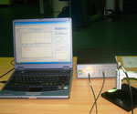
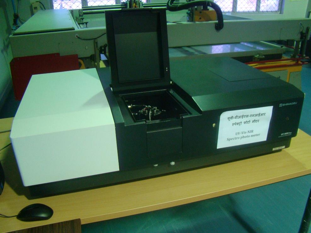
UV/Vis spectroscopy is mainly used in quantitative analysis in analytical chemistry. In the field of material science predominantly used to study the optical properties of materials, such as absorption, transmittance and reflectance of the developing material. Some extend it is used to estimate the energy band gap of semi-conductors. The samples can be finely divided powders, low concentration solutions and solids or thin films.
Centre for Sol-Gel Coatings (CSOL)
Dr. K. Murugan
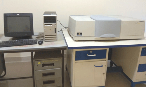
LAMBDA 650 UV/Vis Spectrophotometer
This instrument is ideally suited for all interdisciplinary material and nanoscience applications. Academic or Industrial laboratories can perform various optical analysis on liquids, gels, and solid materials. Applications range from color analysis of paints and textiles, turbid solutions, and enzyme kinetics in life science, biochemistry, pharmaceutical laboratories optical properties of nanoparticles of metal, semiconductors etc. It includes special Universal Reflectance Accessory (URA) assembly, and operates in range of 190-900nm.
Centre for Nanomaterials (CNM)
Dr. Promod H Borse
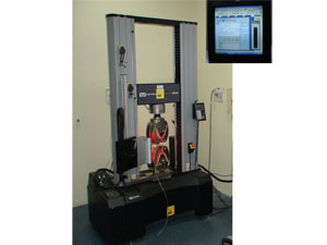
Load applied on test piece: upto 150 kN
This unit is used to study the mechanical properties of materials under tension and compression. The sample to be tested is gripped between the lower fixture of the unit and the upper crosshead and the desired load is applied. The computer interface measures the crosshead movement and the extension/compression of the sample. The unit is equipped with a video extensometer so that the change in dimension of the sample can be measured without any sensors coming in contact with the sample. Extra ports are available for additional devices such as an ultrasonic detector to study grain boundary migration.
Universal Testing machine is for conducting tests like tension, compression, bending, etc., on metals and other materials. The machine is electrically driven and specimen loading is achieved hydraulically. The machine is equipped with pendulum dynamometer recording device for registering load-deformation diagram.
Centre for Engineered Coatings (CEC)
Dr.N. Ravi
Omicron Nano Technology, UK
The instrument has the capabilities of depth profiling by Ar ion etching, Imaging XPS, Auger photoelectron spectroscopy (static and scanning modes), Scanning Electron Microscopy (SEM), Sample heating (upto 100oC) and cooling (liq N2 temp.). The technique being surface sensitive, it is very useful to characterize nanomaterials including, powders and thin films.
Centre for Nanomaterials (CNM)
Dr. Neha Yeshwanta Hebalkar

D8 Advance, Bruker
X-ray diffraction (XRD) is one of the basic tools for material characterisation and is used to obtain structural information on an atomic scale from both crystalline and non-crystalline (amorphous) materials. XRD is a non-destructive technique and can be successfully applied to determine crystal structures of various types of materials such as metals, alloys, ceramics and inorganic compounds, in both the bulk and thin-film/coating forms. XRD also can be applied to obtain structural information such as crystallite size, lattice strain and crystal orientation. The X-ray diffractometer is a versatile instrument for phase and structural analysis of metals, powders and thin-films. The unit at ARCI is equipped with a Cu source and a high speed 1D Lynx Eye detector mounted on a vertical goniometer. This XRD machine can be used to carry out angular dispersive scans with 2 from 5 to 160 deg. and an angular resolution of 0.002 deg. Specially designed sample holders are available for mounting of solid samples with different thicknesses and powder samples on a horizontal spinning (omega) sample stage. For regular powders and other bulk specimens, XRD profiles acquired in (symmetric) geometry, whereas for the thin films and coatings, these profiles are obtained using what is called as grazing incidence XRD (GI-XRD).
Centre for Materials Characterization and Testing (CMCT)
Dr. K. Suresh
